IPS, Waseda University
2-7 Hibikino, Wakamatsuku, Kitakyushushi,
Fukuoka 808-0135 Japan
◆Research
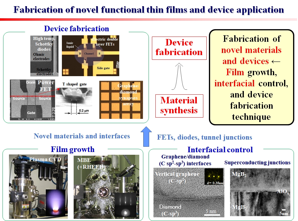
We have been developing novel thin films, especially novel brain-mimic materials and devices,
that can innovate our information society, by using thin film growth technique
Recently, we have mainly been fabricating novel materials and devices by
combining graphene and diamond films. Especially, we are developing image detection
and recognition devices using special photoconducting characters of graphene/diamond heterojunctions.
We are also devloping next-generation semiconductor power devices using diamond semiconductors.
Recent research topics
〇 Carbon semiconductor electronics
・Development of novel AI devices using diamond/graphene heterojunctions
(Brain-mimic novel light sensing devices,
such as for image recognition and time-series data prediction
(Research on the boader line between information and electronics engineering)
・Development of high-performance power devices using diamond semiconductors
(High-power operation devices far surpassing existing materials)
(Research on electronics and materials engineering)
バナースペース
Ueda Lab.
2-7 Hibkino, Wakamatsuku,
Kitakyushushi, Fukuoka 808-0135, JAPAN
TEL: +81-93-692-5176
E-mail:k-ueda[AT]waseda.jp
(Swap [AT] with @)