・Multibit optoelectronic memory using diamond/graphene (C sp3-sp2) junctions
The CNW/diamond photomemristors (Fig. 1) also show apparent response to optical pulses (Fig. 2).
The output current (conductivity) was increased in proportion to the number of optical pulses
under positive bias and decreased under negative bias. The numer of levels and heights of
the curren steps can be controlled by changing optical pulse intensity, pulse width, bias voltage, etc.
These results indicate that CNW/diamond photomemristors can be used as multibit optoelectronic memory,
where information is stored as multilevel resistance in a nonvolatile manner.
(Ref.: K. Ueda et al. Appl. Phys. Lett. 117 (2020) 092103; Dia. Relat. Mater, 34 (2019) 626)
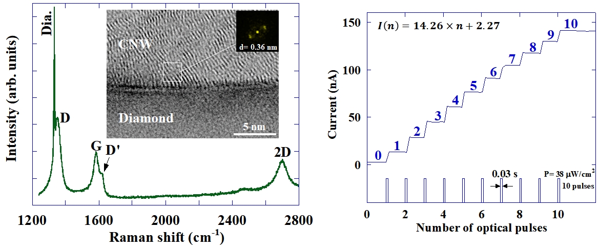
Left fig.:Raman and TEM results for graphene/diamond junctions. Right fig. :Pulse right dependence of the junctions (10 pulses).