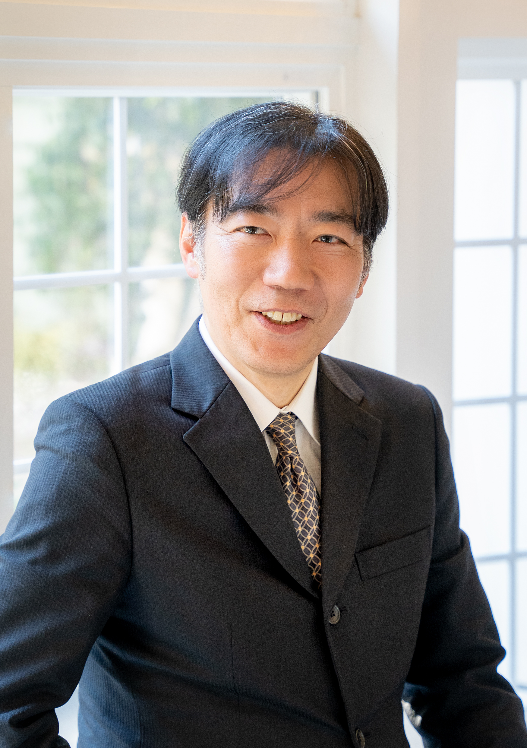

・Mar. 1996 Master of Science, Osaka University
・Mar. 1996 - Jan. 1997 Toshiba Company, researcher
・Mar. 2000 Dr. of Science, Osaka University
・Apr. 2000 - Jan. 2001
ISIR-sanken, Osaka-University, post doctoral fellow
・Feb. 2001 - Mar. 2009
NTT Basic Research Laboratories, researcher
・Apr. 2009 - Mar. 2021
Graduate school of engineering, Nagoya-Univ,
Assoc Professor
(Mar.-Aug. 2011 Invited researcher;
Neel Institut, CNRS, France)
・April 2022 -
Graduate school of IPS, Waseda University
Professor
1. Carbon electronics (diamond, graphene) (2005-)
2. Topological materials and devices (2018-)
3. Heusler spintronics (2010-)
4. Oxide electronics (2009-2018)
5. Superconducting properties of MgB2 films (2001-2005)
6. Magnetic and electronic properties of oxides (1997-2001)
Functional thin films laboratory
Graduate school of information, production and systems
Waseda University
![]() Kenji Ueda /k-ueda[AT]waseda.jp (please swap [AT] with @)
Kenji Ueda /k-ueda[AT]waseda.jp (please swap [AT] with @)
1. Highly accurate recognition of handwritten digits by using photomemristive
properties of graphene/diamond heterojunctions
H. Iwane and K. Ueda
Jpn. J. Appl. Phys., 65 (2026) 061003-1-6
2. Diamond/graphene (carbon sp3-sp2) heterojunctions for neuromorphic device
applications
H. Iwane, G. Saito, S. Muto, and K. Ueda
J. Mater. Res., 39 (2024) 2107-2114. (Invited feature paper).
3. Physical reservoir computing using vertically aligned graphene/diamond
photomemristors
Y. Ito, H. Iwane, S. Jia, and K. Ueda
Applied Physics Express, 16 (2023) 071004-1-5
4. Optoelectronic synapses using vertically aligned graphene/diamond heterojunctions
Y. Mizuno, Y. Ito, and K. Ueda, Carbon, 182 (2021) 669-676.
(Press release (21.7.2))
(Appeared in 電波新聞(DEMPA DIGITAL)(7/9)、マイナビニュースTECH+(7/6),
つくばサイエンスニュース, わかる科学 (8/15))
<To Publication list>